

D'classified Audio (Mixed Signal)
Abstract
Abstract
Google Meet Link: https://meet.google.com/qij-xqxg-eow
1: Introduction
Have you ever wondered how your phone or laptop can play loud, clear music without getting hot, even though it is driving powerful speakers? Or how modern Bluetooth speakers can run for hours on a battery and still sound great?
The secret behind this is a special kind of amplifier called a Class-D audio amplifier. Unlike traditional amplifiers that waste a lot of power as heat, a Class-D amplifier works more like a smart switch: it rapidly turns transistors ON and OFF and uses clever filtering to convert these fast digital-looking signals back into smooth analog sound.
In this project, we’ve built our own Class-D audio amplifier from scratch - but in a modern and exciting way. The “brain” of our amplifier is an FPGA, which generates a high-speed digital PWM signal that represents music. This digital signal then drives a MOSFET power stage, and finally an LC filter turns the switching waveform back into real, smooth audio that drives a speaker.
2: Methodology
2.1: System Architecture
The design was divided into two subsystems, a digital PWM generation block (FPGA) and an analog power stage with output filtering, which were integrated in the final stage.
2.2: Digital Block - PWM Generation
- A sine wave was sampled at 50 kHz, stored as 256 8-bit values in FPGA BRAM.
- A 195 kHz sawtooth counter was compared against the sine values to generate the PWM output.
- Two complementary outputs with 120 ns dead-time were mapped to Pmod pins of the Nexys4 DDR board.
2.3: Analog Block - Power Stage & Filter
- An NMOS half-bridge switched a 12V supply according to the incoming PWM, producing an amplified 0–12V PWM.
- An IR2110 gate driver was used to properly interface the FPGA output with the MOSFET gates.
- A 2nd-order LC low-pass filter (L = 22uH, C = 1.5uF) recovered the sine wave, and a DC-blocking capacitor removed the output offset.
2.4: Simulation & Testing
- Digital block verified via Verilog testbench; analog block simulated in LTSpice.
- Final integration tested on a breadboard with oscilloscope verification for PWM generation stage.
3: Component & Analysis
3.1: Nexys4 DDR FPGA Board (Artix-7)
An FPGA is essentially a chip that you can program to behave like any digital circuit you want. Unlike a microcontroller that runs code sequentially, an FPGA executes everything in hardware and in parallel, making it much faster for signal processing tasks. The Nexys4 DDR is built around Xilinx's Artix-7 FPGA and comes with a 100 MHz onboard clock, built-in BRAM, and plenty of I/O. In this project, it handles the entire digital side, storing the sine wave lookup table, running the sawtooth counter, and generating the PWM output at 195 kHz.
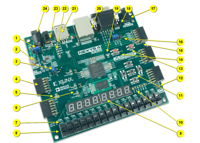
Figure 1: Nexys 4 DDR Artix-7 FPGA Board
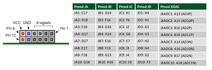
Figure 2: Pmod Interface Connection and Pin Mapping
Pmod Ports
The Pmod ports on the Nexys4 DDR are 12-pin headers that expose the FPGA's GPIO pins to the outside world. Each port has 8 logic signal pins along with 3.3V and GND pins, making them the most straightforward way to get signals out of the FPGA onto a breadboard.
Precautions:
- Pmod pins operate at 3.3V (LVCMOS33) - never feed a higher voltage back into them.
- Always ensure the FPGA and breadboard share a common ground before powering up.
3.2: IRF540N MOSFET (M1, M2)
A MOSFET is a voltage-controlled switch, apply enough voltage to the gate and it turns on, connecting drain to source. The IRF540N is an N-channel power MOSFET, chosen for its low on-resistance and fast switching speed, both of which matter a lot in a Class-D amplifier running at high switching frequencies.
Half-Bridge Setup
The two MOSFETs are arranged in a half-bridge configuration, the core power switching stage of the amplifier. The structure is straightforward:
- M1 (high-side) sits between 12V and the output node
- M2 (low-side) sits between the output node and GND
- The output is taken from the midpoint between them
A natural alternative would be to use a PMOS for the high-side and NMOS for the low-side, and this is actually how many beginner designs are built, since a PMOS on top is easier to drive. However, PMOS devices generally have higher on-resistance and slower switching, which leads to more losses at high frequencies. Using two NMOS devices gives better efficiency and more symmetrical switching behaviour, which is why IRF540N was chosen for both positions.
Operation
The two switches are never ON at the same time. They alternate:
- M1 ON, M2 OFF → output node pulled to 12V
- M2 ON, M1 OFF → output node pulled to 0V
Switching at 195 kHz with a duty cycle that follows the sine wave, the midpoint toggles between 0 and 12V in exactly the pattern of the input PWM, just now at full power. This amplified PWM then goes into the LC filter to recover the audio signal. One consequence of using NMOS on the high side is that M1’s gate needs to be driven above 12V to turn on properly, since its source floats at the switching node. This is handled by the IR2110 gate driver, covered next.
3.3: IR2110 Gate Driver (X1)
A gate driver is essentially a buffer that sits between your control signal and the MOSFET gate. The FPGA output cannot directly drive a power MOSFET because it does not have enough current to charge and discharge the gate capacitance quickly enough for clean, fast switching. The IR2110 solves this by providing high-current gate drive for both high-side and low-side MOSFETs.
The high-side MOSFET (M1) has a floating source that sits at the switching node, which toggles between 0V and 12V. To turn M1 on, its gate needs to be higher than its source. This means we need a voltage above 12V, which we do not directly have. This is the classic bootstrap problem.
The IR2110 handles this using a bootstrap capacitor (C8) and diode (D1):
- When M2 is ON, the switching node is at 0V and the bootstrap capacitor charges up through D1 to ∼12V.
- When M1 needs to turn ON, this stored charge is used to drive the gate above 12V.
- The capacitor keeps refreshing every switching cycle, sustaining the high-side drive.
3.4: IN4148 Diodes (D1, D2, D3)
The 1N4148 is a small, fast-switching signal diode. It is a standard component that is widely used in high-frequency switching circuits because it reacts quickly and handles high-speed transitions efficiently. Three of these diodes are utilized in this design, with each serving a distinct operational purpose within the gate drive circuitry:
- D1 sits in the bootstrap charging path. When M2 is ON and the switching node is at GND, D1 conducts and charges C8 through the 12V supply. It also prevents C8 from discharging back when the switching node rises.
- D2 and D3 sit directly on the gate drive output lines of the IR2110. They clamp any reverse voltage spikes that appear during switching transients, protecting the gate driver outputs from seeing harmful negative voltages.
3.5: Bootstrap & Decoupling Capacitors (C6, C7, C8)
Capacitors in this circuit are utilized for two distinct operational tasks depending entirely on where
they are positioned within the gate drive and switching network.
- C8 (470 μF) (Bootstrap Capacitor): This component makes the high-side floating drive possible. Every time the low-side MOSFET (M2) turns ON, the switching node drops to GND, allowing C8 to charge rapidly up to ∼12V through the bootstrap diode (D1). When M1 needs to turn ON, this stored charge floats upwards relative to the switching node, providing the
vital above-rail voltage needed to drive M1’s gate terminal. Without this charge reservoir, the high-side NMOS simply cannot activate. - C6 (0.1 μF) and C7 (1 μF) (Decoupling Capacitors): These capacitors sit directly adjacent to the VCC and VDD voltage supply pins of the IR2110 driver IC. Every time the power MOSFETs alternate states, rapid transient spikes in current occur which the main power supply distribution lines cannot instantaneously handle. These decoupling capacitors act as local energy reservoirs, absorbing high-frequency electrical noise and stabilizing the supply rails during switching phases.
3.6: LC Low-Pass Filter (L1 = 44uH, C3 = 470uF)
At the output of the half-bridge, you have a high-power PWM signal toggling between 0V and 12V at 195 kHz, with the audio information encoded directly within its duty cycle. The LC filter averages this waveform out and recovers the underlying analog sine wave.
The inductor resists rapid current variations while the capacitor smooths the output voltage voltage changes. Together, they form a 2nd-order passive low-pass filter that rolls off at an aggressive rate of 40 dB/decade, which provides a much steeper and cleaner transition band than a basic single-pole RC filter network.
The characteristic cutoff frequency (fc) of this second-order system is defined by fc = 1/(2pi(LC^1/2)). Given our chosen values of L = 44.4 μH and C = 470 μF, the calculation yields a cutoff frequency of approximately 1.1 kHz. This boundary sits comfortably right above the fundamental voice or target audio band and safely below the 195 kHz switching carrier frequency. Consequently, the
recovered sine wave passes through cleanly while the high-frequency switching carrier components are completely filtered out.
4: Digital Implementation (Verilog)
The digital block consists of four parts:
- Sine LUT (sine rom): A 256-entry lookup table storing one full cycle of a sine wave as 8-bit values (0–255), addressed sequentially to replay the waveform.
- Audio Sampling Counter: Divides the 100 MHz clock down to 50 kHz, which sets the rate at which the LUT address increments, producing a 1 kHz output tone.
- Sawtooth Generator: An 8-bit counter incrementing every 2 clock cycles, generating a 195 kHz ramp that serves as the PWM carrier.
- Comparator & Dead-Time: Sine and sawtooth are compared each clock cycle to generate pwm_raw. A 20-cycle shift register then derives two complementary outputs with 200 ns dead-time, ensuring M1 and M2 are never ON at the same time.
Github Link:
https://github.com/VibhuKavBhat/Mixed-Signal-Class_D-Amplifier
Demo:
https://drive.google.com/file/d/1LKM7AgJ1bsuuK9dtY5xDAgqQom6Fb2kE/view?usp=
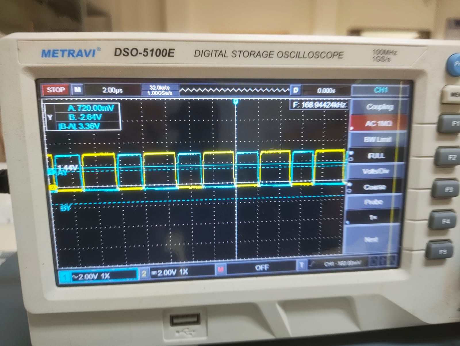
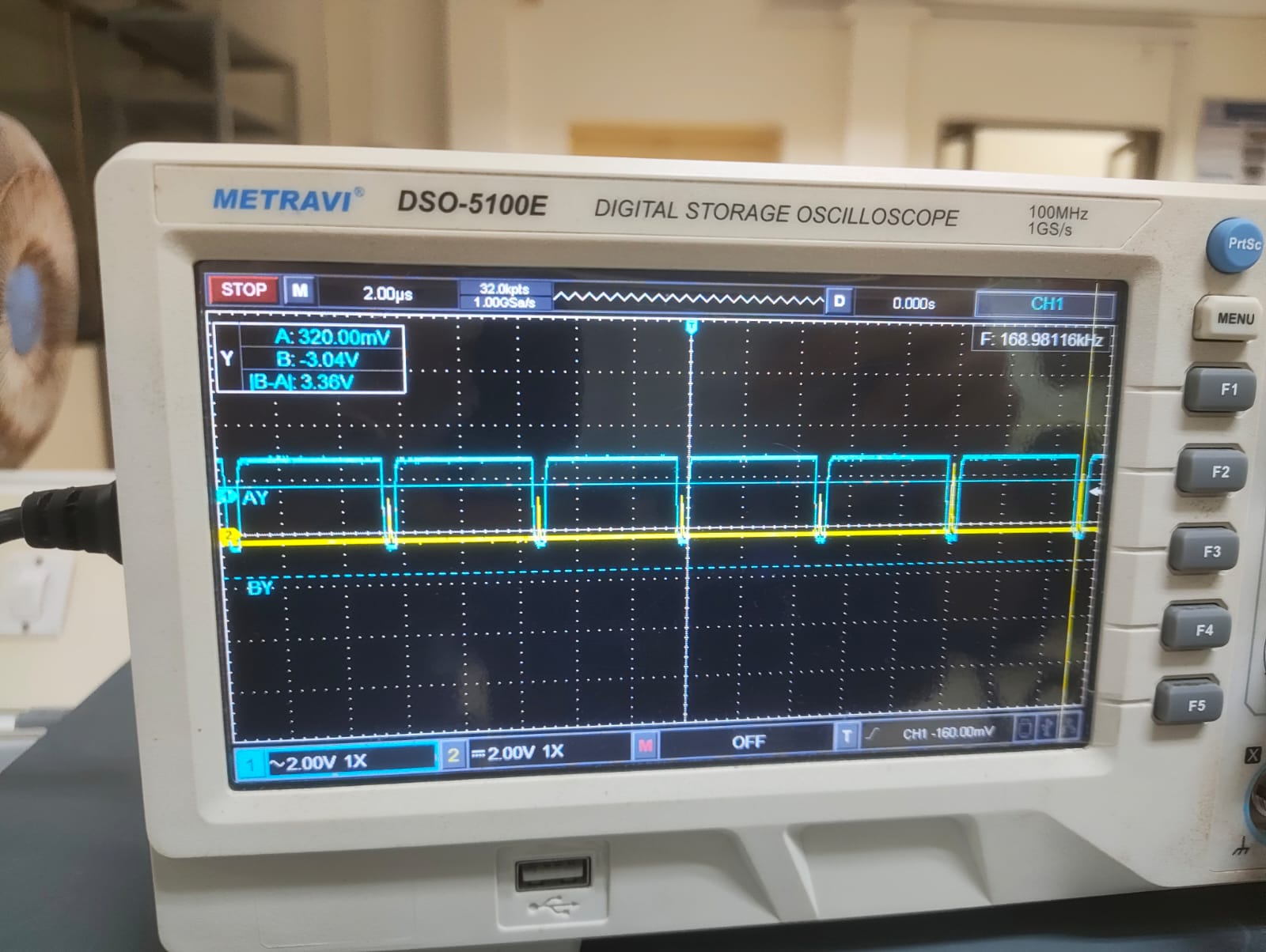
PWM Output Waveforms
5: Analog Implementation (LTSpice)
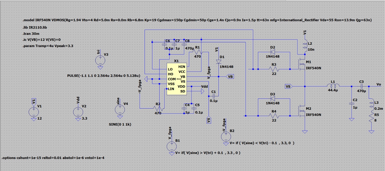
Figure 5: LTSpice Schematic
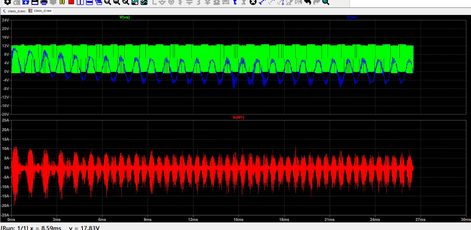
Figure 6: Simulation Waveform Analysis
Demonstration: LC Filter Working
https://drive.google.com/file/d/1Xx9VSeYs9ck7kO-eKn5jJ1ygCyIp4_CX/view?usp=
6. Conclusion
This project successfully demonstrated the design and implementation of a mixed-signal Class-D audio amplifier. The digital block was fully implemented on the Nexys4 DDR FPGA, reliably generating a 195 kHz PWM signal from a sine wave with proper dead-time logic. The analog block was thoroughly verified through LTSpice simulation, confirming correct switching behaviour, bootstrap charging, and a clean sine wave at the output. Due to component availability constraints, the analog stage could not be assembled on hardware.
However, the simulation results closely model real-world behaviour and confirm the design is ready for physical implementation.
Overall, the project built a strong practical understanding of how digital control and analog power stages come together in a real mixed-signal system, with hands-on exposure to tools like Vivado and LTSpice.
7. Limitations and Future Work
Limitations:
- The analog power stage could not be physically assembled due to unavailability of certain components in the lab, and remains a simulation only implementation.
- The LTSpice simulation uses ideal behavioural sources to replicate the FPGA PWM, which may not fully capture real world signal integrity issues.
- The LC filter cutoff of approximately 1.1 kHz sits very close to the audio frequency, which could cause slight attenuation of the output in hardware.
Future Work:
- Assemble and test the analog stage on hardware to validate simulation results.
- Extend the digital block to support real audio input instead of a hardcoded sine wave.
- Optimize the LC filter values for a wider audio bandwidth.
- Explore a full H-bridge configuration for higher output power and true differential drive.
Report Information
Team Members
Team Members
Report Details
Created: May 17, 2026, 10:58 p.m.
Approved by: None
Approval date: None
Report Details
Created: May 17, 2026, 10:58 p.m.
Approved by: None
Approval date: None