

FSM-Based Digital Signal Generator
Abstract
Abstract
Google meet link -https://meet.google.com/mpi-jygr-bmb
Aim
To design, implement, and verify a Finite State Machine (FSM)-based digital signal generator in Verilog HDL that outputs four distinct waveforms (Square, Sawtooth, Triangle, and Sine) selectable via a 2-bit control input, operating within an 8-bit resolution and a 256-clock period, suitable for FPGA deployment.
Introduction
Digital signal generators are foundational building blocks in embedded systems, communications hardware, and test equipment. Unlike their analog counterparts, digital generators offer inherent precision, repeatability, and ease of integration with digital control logic. By representing waveforms as sequences of numeric samples output at regular clock intervals, they can be synthesised directly on programmable devices such as FPGAs.
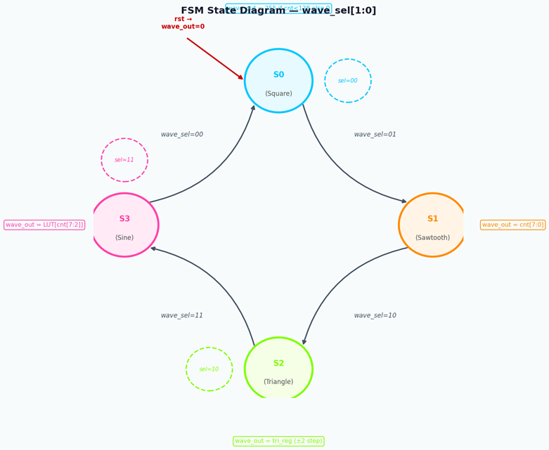
This project implements a waveform generator using a Finite State Machine architecture in Verilog HDL. The FSM acts as a registered multiplexer, selecting one of four generation strategies based on a 2-bit wave_sel control input and updating the 8-bit wave_out output on every positive clock edge. The design targets simplicity, glitch-free operation, and clean timing behaviour within a single clock domain.
Literature Survey and Technologies Used
Background
FSM-based datapath control is a well-established technique in digital design. Moore and Mealy machine models provide a formal framework for state-driven output generation. The use of Look-Up Tables (LUTs) for sine approximation in resource-constrained environments is described in standard FPGA design references and is employed here for the sine waveform output.
Technologies Used
- Verilog HDL (IEEE Std 1364) - RTL hardware description language
- FSM - Moore machine model; registered state logic for glitch-free, deterministic outputs
- 8-bit unsigned arithmetic - all waveform outputs in range [0–255]
- 64-entry ROM LUT - sine approximation, indexed via counter[7:2]
- Verilog HDL simulation - functional verification across 512 samples
- Single-clock FPGA synchronous design - no CDC logic required
Methodology
System Architecture
The top-level module instantiates a single FSM module receiving: a system clock (clk), active-high reset (rst), a 2-bit waveform selector (wave_sel[1:0]), and driving an 8-bit output (wave_out[7:0]). An internal 8-bit counter increments every clock cycle and is used to derive all sample values.
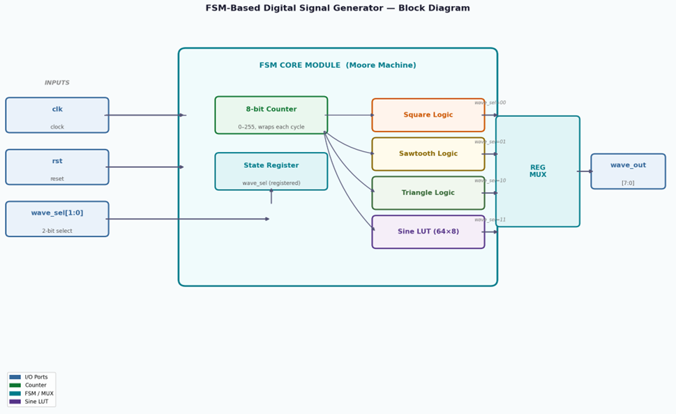
Waveform Generation Strategy
- Square Wave - wave_out = 255 when counter < 128, else 0. Produces 50% duty cycle.
- Sawtooth Wave - wave_out = counter[7:0]. Natural 8-bit rollover every 256 clocks.
- Triangle Wave - wave_out increments by +2 (0→252) then decrements by −2 (252→0). Peak is 254 due to ±2 step-size boundary.
- Sine Wave - 64-entry LUT addressed by counter[7:2] yields 8-bit sine samples, each held for 4 clock cycles.
Results
The design was verified through Verilog HDL simulation. All four waveforms were captured over 512 samples across the full 8-bit amplitude range. Simulation output and measured parameters are shown below.
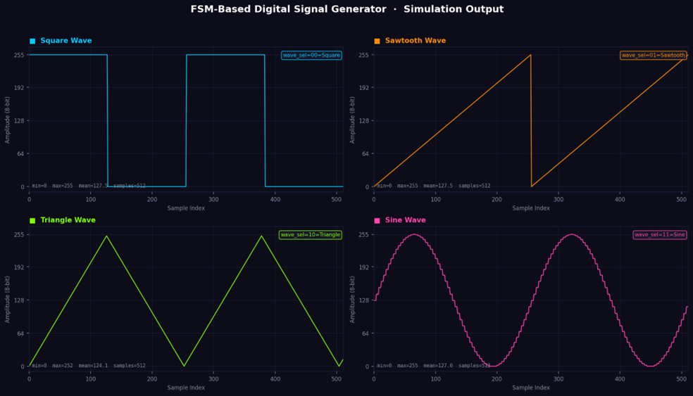
Table I - Measured Waveform Parameters
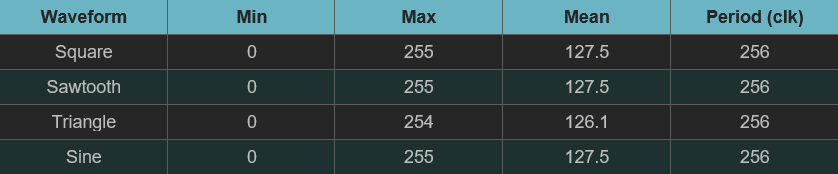
All waveforms operate over the full 8-bit range (Triangle peaks at 254 due to step-size-2 constraint). The 50% duty cycle of the Square wave and symmetry of both Triangle and Sine outputs were confirmed visually and numerically. No spurious transients were observed at state transitions.
Conclusions and Future Scope
Conclusions
The FSM-based digital signal generator was successfully designed, implemented in Verilog HDL, and verified through simulation. All four target waveforms display correct amplitude, period, and symmetry. Registered FSM outputs, a single clock domain, and synchronous-style reset ensure clean, glitch-free operation ready for FPGA deployment.
Limitations
- Triangle peak is 254 (not 255) - intentional artefact of ±2 step-size boundary.
- Sine output is a 64-step staircase approximation; higher fidelity requires a larger LUT.
- One pipeline clock of latency between wave_sel change and wave_out update.
Future Scope
- Increase sine LUT to 256 entries for smoother, lower-distortion output.
- Add a PWM output stage and RC filter for analogue waveform reconstruction.
- Parameterise frequency via a configurable clock divider.
- Deploy on physical FPGA and verify outputs on an oscilloscope.
- Add UART/SPI interface for run-time waveform and frequency selection.
References
- IEEE Std 1364-2005 - IEEE Standard for Verilog Hardware Description Language
- Pong P. Chu, FPGA Prototyping by Verilog Examples, Wiley, 2008
- Xilinx UG901 - Vivado Design Suite User Guide: Synthesis
GitHub Link
GitHub Repository: https://github.com/prajna-hr/FSM-Based-Digital-Signal-Generator
Mentors and Mentees Details
Mentors
Prajna H R
Yahaswi Malepati
Gudise Divya Keerthi
Mentees
Aprameyan R
Shravani Kolage
Mehek SK
Parth Maheshwari
Report Information
Report Details
Created: May 17, 2026, 10:05 p.m.
Approved by: None
Approval date: None
Report Details
Created: May 17, 2026, 10:05 p.m.
Approved by: None
Approval date: None