

NexusV: A RISC-V based SoC on FPGA
Abstract
Abstract
Aim
This project aims to bring-up a fully functional, RISC-V compliant SoC on the Nexys 4 DDR FPGA. Specific objectives include:
- Operating a PicoRV32 processor core at 100MHz.
- Interfacing external hardware, specifically an onboard accelerometer and a temperature sensor, via a memory-mapped SPI controller.
- Driving an external display using a custom VGA controller running on a 25MHz pixel clock.
- Developing a robust firmware architecture that utilizes a hardware bootloader to dynamically load and execute custom, user-written C applications (app.c).
Introduction
The popularization of the open-source RISC-V Instruction Set Architecture (ISA) has opened up silicon design to many, allowing for the creation of highly customized processors. Nexus-V leverages this ecosystem to build a lightweight, scalable SoC from the ground up, avoiding proprietary, vendor-locked microcontrollers. By implementing standard communication protocols over an AMBA AXI4-Lite interconnect, the SoC serves as a flexible foundation for sensor integration and real-time data processing. The project also bridges the gap between digital hardware design and embedded software engineering by providing a platform where firmware enthusiasts can easily deploy custom programs onto a custom silicon architecture.
Technologies used
- Target Hardware: Digilent Nexys 4 DDR (Xilinx Artix-7 FPGA).
- Processor Core: PicoRV32 (AXI4-Lite wrapped, 32-bit RV32I architecture).
- System Clocks: 100MHz main CPU clock, 25MHz VGA pixel clock.
- On-Chip Memory: 32KB Block RAM (BRAM).
- Peripherals: SPI (interfacing Accelerometer sensor), I2C (interfacing Temperature Sensor), UART (baud rate 115200), VGA monitor interface.
- Hardware Description Languages: Verilog
- Software Stack: C (Firmware, User Applications), RISC-V GNU GCC Toolchain, GNU Make.
- EDA Tools & Automation: Xilinx Vivado, Tcl, Python (serial upload scripts).
Methodology
The development of the SoC was divided into hardware architecture, sensor integration, and software stack development:
A. Hardware Architecture & Clocking:
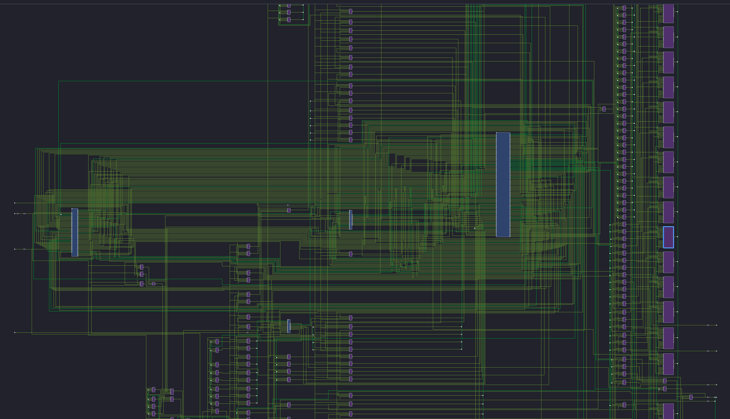
The PicoRV32 core was instantiated as the central bus master and bridged to an AXI-Lite crossbar. The system utilizes mixed clock modes to generate a 100MHz system clock for the CPU and AXI bus, and a separate 25MHz clock domain specifically for the VGA display controller. A 32KB Block RAM module was synthesized and mapped to the AXI bus to serve as unified instruction and data memory.
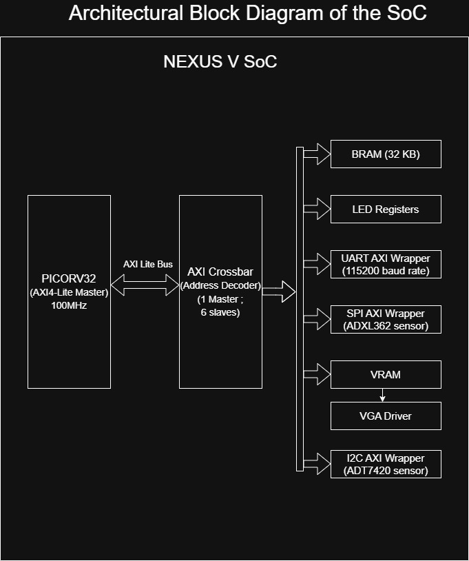
B. Peripheral and Sensor Integration:
Standard IP cores were wrapped in custom AXI-Lite controllers. This memory-mapped approach allowed the CPU to control the hardware by reading and writing to specific 32-bit memory addresses.
SPI: Configured to communicate with the onboard ADXL362 accelerometer and the external temperature sensor.
I2C: Instantiated as a two-wire serial master to support lower-speed, addressable external peripherals. The memory-mapped controller manages the serial clock (SCL) and bidirectional data (SDA) lines, allowing the RISC-V core to easily poll multi-device sensor arrays on a shared bus.
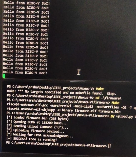
UART: Implemented as the primary communication bridge between the SoC and the host PC. Operating at a 115200 baud rate, the UART RX line is critical for the custom bootloader to receive dynamic .hex firmware payloads, while the TX line provides real-time debug logging and application output to a serial terminal.
VGA: A custom display controller uses the 25MHz clock to generate horizontal and vertical sync signals to drive an external monitor.
C. Firmware Architecture (The Two-Stage Boot):
To avoid reprogramming the FPGA for every software change, the system uses a dual-firmware approach separated by custom Linker scripts (.ld) and Assembly startup files (.s):
Stage 1 (The Bootloader): The boot.c program and its linker script map this code to memory address 0x00000000. The assembly startup file (boot_start.s) initializes the stack pointer and jumps to the bootloader's main function. This code is permanently baked into the FPGA's BRAM during Vivado synthesis. Upon reset, it initializes the UART, listens for a new .hex payload from the PC, writes it to an offset memory location (e.g., 0x00001000), and jumps the CPU to that address.
Stage 2 (User Application): The main user logic (app.c) is compiled entirely separately. Its linker script (app.ld) ensures the compiled instructions start at the offset address expected by the bootloader.
This architecture successfully allows multiple, custom user programs to be written, compiled, and uploaded dynamically in seconds.
Results
The Nexus-V architecture was successfully synthesized, routed, and deployed to the Artix-7 Nexys 4 DDR board. The dual-stage bootloader correctly routed UART payloads to BRAM, allowing continuous software iteration.
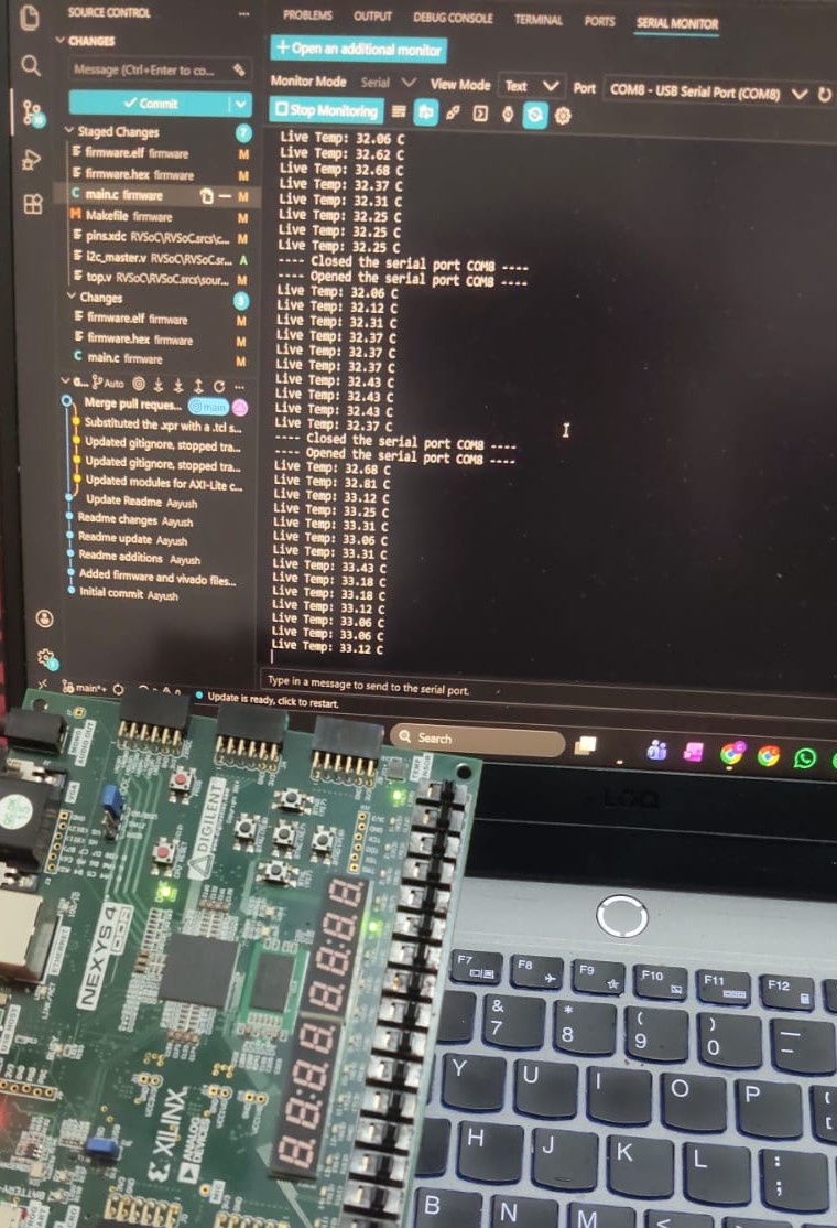
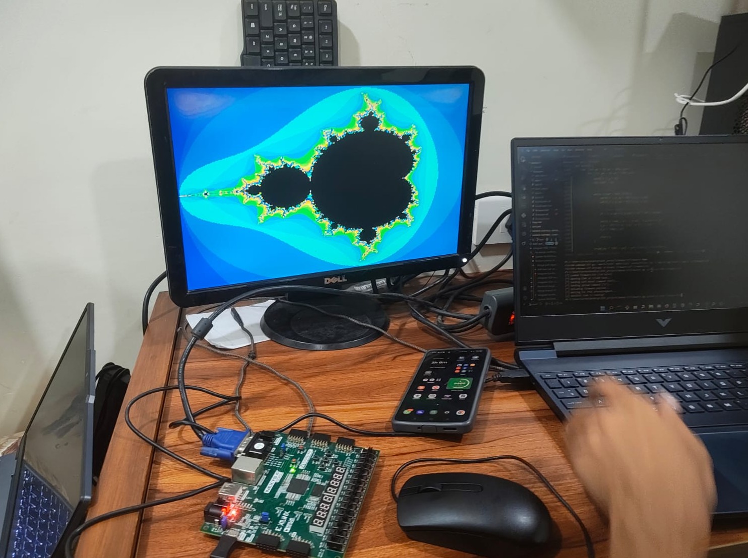
 The images above display a variety of programs that can be run.
Hardware Implementation & Resource Utilization:
LUTs (Look-Up Tables): 1969 / 63,400 (3.1 %)
Flip-Flops (Registers): 1912 / 126,800 (1.5 % )
BRAM (Block RAM Cells): 40 / 135 (29.6 %)
Conclusions
The Nexus-V project successfully demonstrates the end-to-end development of a custom RISC-V microcontroller. By successfully abstracting the hardware layer through a custom bootloader, the FPGA essentially functions as an accessible development board (similar to an Arduino), where users can quickly write and execute custom C programs to read accelerometer and temperature data, outputting results via UART or VGA.
Future Scope
The modularity of the AXI bus lays a strong foundation for future hardware expansions. Potential upgrades include adding hardware-accelerated Digital Signal Processing (DSP) blocks, expanding the BRAM via an external DDR memory controller, or adding a FreeRTOS port for real-time multitasking.
References/ GitHub Repo
GitHub Repository: https://github.com/Shiken56/Nexus-V
PicoRV32 Repo: https://github.com/YosysHQ/picorv32
Acknowledgements
As executive members of IEEE NITK, we are incredibly grateful for the opportunity to learn and work on this project under the prestigious name of the IEEE NITK Student Chapter.
Report Information
Team Members
Team Members
Report Details
Created: April 7, 2026, 10:29 p.m.
Approved by: None
Approval date: None
Report Details
Created: April 7, 2026, 10:29 p.m.
Approved by: None
Approval date: None